�Ӱ�ԭ�� researchers �����Ի��� are part of an international collaboration that has demonstrated a new way to manipulate and measure subtle atomic vibrations in nanomaterials. This breakthrough could make it possible to develop customized functionalities to improve on and build new technologies.


Electron beams in powerful microscopes have probed materials and nanostructures with atomic-scale resolution, imaged the atomic arrangements and, in combination with theory, unveiled electronic and magnetic properties. Recent developments in microscopy help make it possible to get direct signals from phonons, namely vibrational modes, with high resolution in both space and energy. Researchers can now measure distinct vibrational modes at interfaces in multilayered structures, defects, and other inhomogeneities.
“Our team combined such measurements with laser probes and theoretical investigations to obtain a complete picture of the underlying physics that ultimately will form the basis of new technologies,” Pantelides said.
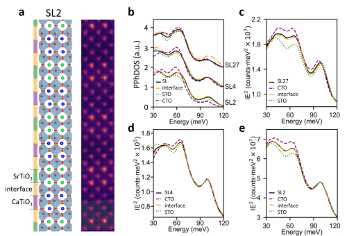
In this research, published in the journal Nature on Jan. 26, the team layered two different oxides into a Lego-like nanostructure called a superlattice. The structures were imaged at the atomic scale by , the paper first author and a researcher at the University of Virginia. (Ph.D.’16), a former student of Pantelides and an expert microscopist at the Center for Nanophase Materials Sciences at Oak Ridge National Laboratory, performed the precision measurements of vibrational modes of these complex superlattices.
Caldwell, Flowers Family Chancellor Faculty Fellow in Engineering and associate professor of mechanical engineering, and his student Joseph Matson performed complementary infrared spectroscopies of the vibrational modes. Pantelides, University Distinguished Professor of Physics and Engineering, William A. and Nancy F. McMinn Professor of physics and professor of electrical engineering, and his group members Andrew O’Hara and De-Liang Bao, research assistant professor and postdoctoral scholar, respectively, performed the theoretical calculations that provided links between diverse experiments to construct a comprehensive picture. The combined research established that as the thickness of the layers in the superlattices shrinks, the atomic vibrations are initially dominated by those of the two bulk materials, but gradually evolves to be dominated by the atomic interfaces, which define a new crystal structure.
WHY IT MATTERS
“Any time there is a structure with new properties, the engineering mind goes straight to thinking of what new materials with novel functionalities and new devices can be made. Simply put, this is how technology gets created.”
Earlier combinations of theoretical calculations using quantum mechanics with physical experiments allowed physicists and engineers to understand how materials behave. Such investigations resulted in the creation and development of the digital devices we take for granted today. Electron microscopes played a major role in these quests, but, until recently, they did not have sufficient resolution to image atomic vibrations.
“Emergent properties result at the nanoscale, especially when we put materials together. From these combinations we get new behaviors that we didn’t expect,” Pantelides said. “Any time there is a structure with new properties, the engineering mind goes straight to thinking of what new materials with novel functionalities and new devices can be made. Simply put, this is how technology gets created.”
Caldwell and Matson have been investigating the infrared properties of atomic-scale superlattices. “The infrared properties of polar crystals are primarily driven by the optical phonons of the materials. Thus, this work builds on a concept we refer to as the crystalline hybrid, where combinations of atomically thin materials in superlattices can be used to induce emergent properties,” Caldwell said. This effort was significantly enhanced by demonstrating that the scale of these measurements can be shrunk to measure the most precise behavior captured to date.
WHAT’S NEXT
This work has the potential to improve knowledge across microscopy, optical science, physics and engineering. “We have reached a step change in this technology. By improving how we measure, we are able to better work with and manipulate these nanomaterials. We are much more confident that we can design structures with custom properties,” Pantelides said.
Pantelides and Caldwell will continue collaborating with Oak Ridge National Laboratory to pursue more advances in the field, especially in expanding to different crystal structures and other material systems of interest such as nitride-based semiconductors.
FUNDING
Pantelides’ contributions at �Ӱ�ԭ�� were supported by the U.S. Department of Energy, Office of Science, Basic Energy Sciences, Materials Science and Engineering Directorate grant number DE-FG02-09ER46554 and by the McMinn Endowment. Caldwell contributions were supported by the National Science Foundation Division of Materials Research award number 1904793.
GO DEEPER
The article, “” was published in the journal Nature on Jan. 26.
Researchers from the University of Virginia, Sandia National Laboratory, University of California Berkeley, Purdue University, and Humboldt University and the Paul-Drude-Institut fur Festkörperelektronik in Germany participated in this research.